
CMP Process Development & Services
Accelerate Your CMP Process with the Entrepix CMP Foundry
Entrepix provides CMP process services, CMP process development, CMP consulting, process optimization, consumable evaluation and outsourced CMP processing for semiconductor and advanced-material applications.
Our experienced applications team combines extensive CMP process knowledge with dedicated development equipment, advanced wafer cleaning and metrology capabilities to help customers solve challenging planarization problems, shorten development cycles and reduce risk.
From determining initial CMP feasibility to developing and validating a complete process of record (POR), Entrepix provides the expertise and infrastructure needed to move your process forward

How can the Entrepix CMP Foundry help?
Every CMP challenge is different. Materials, device structures, consumables, equipment, cleaning requirements and performance targets all influence the final process.
Entrepix works collaboratively with customers to develop new CMP processes, optimize existing processes and evaluate potential solutions. Our extensive process experience and dedicated R&D environment allow experimentation and process iteration without tying up valuable customer production equipment.
CMP Process Services Built Around Your Application
CMP Process Development
Develop and validate CMP processes for challenging materials, device structures and emerging applications.
CMP Process Optimization
Improve removal rate, uniformity, defectivity, surface quality, cleaning performance and overall process stability.
CMP Consulting
Access experienced CMP applications support for process troubleshooting, technical review and optimization.
Consumable & Hardware Evaluation
Conduct controlled, head-to-head evaluations of slurries, pads, post-CMP cleaning chemistries, hardware and other process variables.
Feasibility Testing & POR Development
Determine whether new materials and structures can successfully withstand CMP processing, then develop and validate an optimized process of record.
Outsourced CMP Production
Access qualified CMP processing for development programs, startups, pilot production or applications where internal capacity is constrained.
From CMP Challenge to Process of Record
A Structured Path to CMP Process Development
Successful CMP process development requires more than identifying a polishing recipe. Entrepix evaluates the interaction between the substrate or device, tool configuration, consumables, chemistry, cleaning processes and performance requirements to develop a solution around your specific application.
Define Requirements
Materials
Device Structure
Integration Constraints
Performance Targets
Develop
CMP Equipment
Slurry & Pad
Chemistry
Process Parameters
Validate
Removal & Uniformity
Defectivity
Surface Quality
Post-CMP Clean & Metrology
Scale
Process of Record
Qualification
Process Transfer
Production / iFlow
CMP Applications & Materials
Extensive CMP Process & Materials Experience
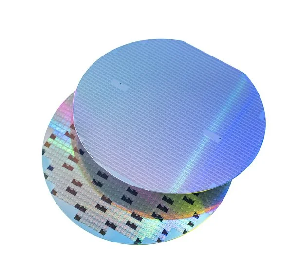
Entrepix has developed CMP expertise across traditional semiconductor processes as well as emerging applications, compound semiconductors and advanced substrate materials. This broad knowledge base can reduce the amount of initial discovery required when developing a new process.
Traditional CMP
- Oxide
- Tungsten
- Copper
- Barrier Metals
- STI
- Polysilicon
- Low-k Dielectrics
- Ultra-Low-k Dielectrics
- Metal Gates
- High-k Dielectrics
- Aluminum
- Analog & RF
- ILD
- TSV
Advanced & Emerging Applications
- Advanced Packaging for AI
- Photonics & Waveguides
- MEMS
- µLED
- Quantum Computing
- Direct Wafer Bonding
- Ultra-Thin Wafers
- Power Devices
- Detector Arrays
- LED & Optics
- Novel / More-than-Moore Devices
Advanced Substrates & Materials
- Silicon & SOI
- InP & InGaP
- GaAs & AlGaAs
- GaN
- SiC
- SiGe
- Sapphire
- Diamond & DLC
- Lithium Niobate / Tantalate
- Quartz & Glass
- AlN on Silicon
- GaN on Silicon
CMP Foundry Capabilities
Develop Using Production-Relevant CMP Infrastructure
Developing a successful CMP process requires the ability to polish, clean, characterize and iterate. The Entrepix CMP Foundry combines CMP equipment, post-CMP cleaning and metrology capabilities in a dedicated development environment.
Production-Relevant CMP Platforms
IPEC 472
CMP equipment supporting process development, optimization, testing and qualification.
Post-CMP Cleaning
Advanced post-CMP wafer cleaning capability for integrated CMP and cleaning process development.
Dedicated CMP Foundry
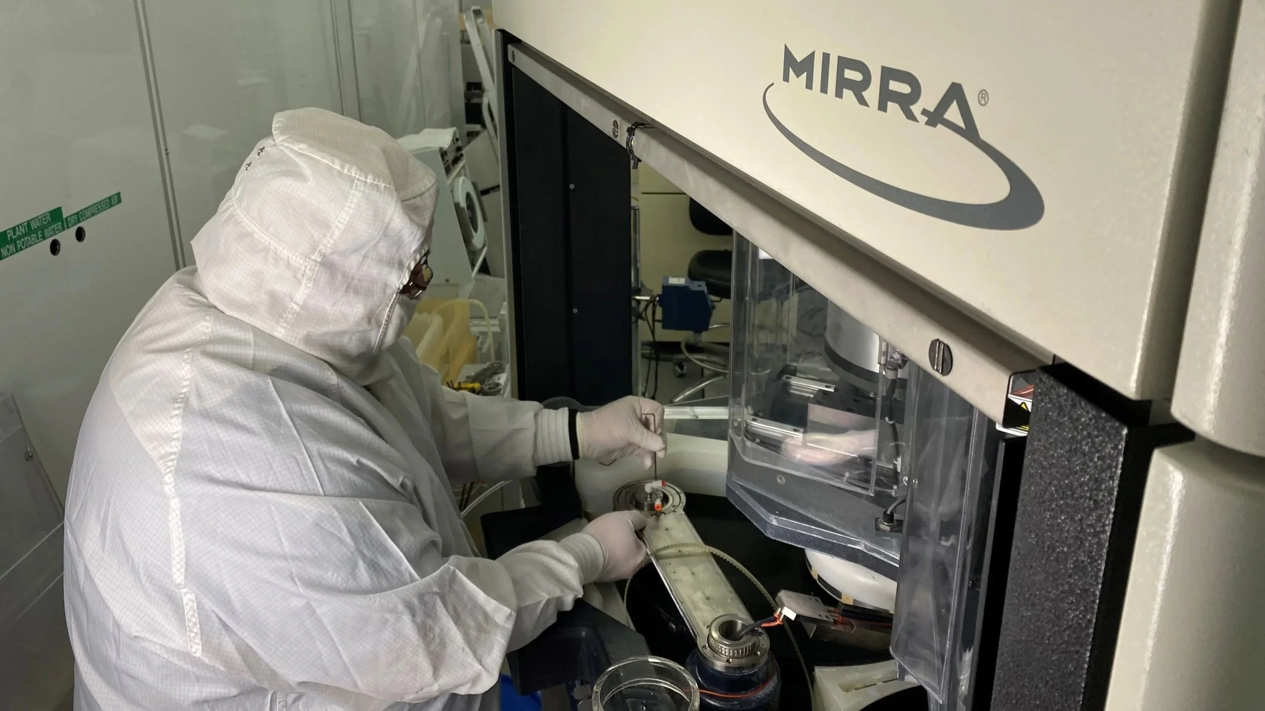
Dedicated cleanroom environment for CMP process development, consumable evaluation and testing.
Measure & Validate Results
Accelerate Your Path to POR
50+ YEARS
CMP & Clean Experience
EXTENSIVE CMP PROCESS PORTFOLIO
Start from existing knowledge, not zero
DEDICATED R&D FACILITY
Develop without consuming production capacity
ZERO CMP CAPITAL INVESTMENT
Access equipment, expertise and metrology as needed
iFab™ Integrated & Distributed Process Services
When Your Process Doesn't Stop at CMP
Many semiconductor and advanced-material development programs require multiple specialized process steps beyond CMP and post-CMP cleaning. Coordinating those capabilities across different suppliers can add time, complexity and risk to the development process.
iFab™ extends Entrepix CMP Process Services beyond the Foundry by connecting core CMP, wafer cleaning and metrology capabilities with complementary semiconductor process resources. Customers can engage Entrepix for a single process step or for broader coordination of a distributed process flow.
The result is a more integrated approach to process development, allowing your team to focus on the application while Entrepix helps coordinate the processing required to move from concept toward a qualified process.
CMP + POST-CMP CLEANING
Wafer Acquisition
Edge Rounding
Analysis
Wafer Bonding
& Backgrinding
Ready to Solve Your Next CMP Challenge Faster?
Whether you’re developing a process for a new material, optimizing an existing CMP process, evaluating consumables or preparing to scale, Entrepix provides the expertise, equipment and process-development resources to help you get there faster and with less risk.
Let’s turn your CMP challenge into a production-ready process.